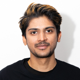
Ing. Swaroop Badekara
Angestellt, Analog/Mixed Signal Design Engineer, pmdtechnologies ag
Abschluss: Master of Science, Technische Universität Chemnitz
Siegen, Deutschland
Werdegang
Berufserfahrung von Swaroop Badekara
Bis heute 3 Jahre und 3 Monate, seit Apr. 2021
Analog/Mixed Signal Design Engineer
pmdtechnologies ag
Design of High performance ADC for CMOS image sensors.
7 Monate, Okt. 2017 - Apr. 2018
Master Thesis in first order 10-bit Sigma Delta ADC in 0.18 um technology.
TU Chemnitz– The full delta sigma design includes DS modulator and Sinc2 decimation filter. – Design of switched capacitors, OTA, high speed clocked comparators, D-flip flops, adders, averagers, hold registers etc., – Non-ideal effects have been investigated in accordance with different feedback topology an their impact quantified. – Performing Montecarlo/corner simulations for further analysis.
4 Monate, Mai 2017 - Aug. 2017
Project Work in Integrated circuit design K-Delta-1-Sigma-Modulator
TU ChemnitzThe main objective of the task was to design a 2 MHz bandwidth, K-path deltasigma (KD1S) converter with 6-bit ENOB. – New concept of sharing the op-amp across K-paths to realize a (KD1S) topology.
10 Monate, Juni 2016 - März 2017
Research Project Software controlled reliability testing of RF MEMS switches.
Fraunhofer ENAS
– Worked on Creating an approach/concept to a software solution to enable a software controlled reliability test of RF MEMS switches. – Designing test setups for component level measurements, switching parameters, lifetime calculations, contact resistance degradation etc.
Ausbildung von Swaroop Badekara
Bis heute 5 Jahre und 9 Monate, seit Okt. 2018
High performance ADC for CMOS Image sensor
Universität Siegen
3 Jahre und 6 Monate, Okt. 2014 - März 2018
Micro and Nano Systems
Technische Universität Chemnitz
Micro-system Design, Advance Integrated Circuit Technology, CMOS VLSI Design, Micro and Nano Devices and Reliability Engineering.
4 Jahre, Aug. 2010 - Juli 2014
Electronics and Communication Engineering
Visvesvaraya Technological University
CMOS VLSI, Analog and Mixed Mode VLSI Design, Linear IC’s, Analog Electronic Circuits, Digital signal processing and Signals & Systems
Sprachen
Deutsch
Gut
Englisch
Muttersprache
Hindi
-
